





In July, one of the most important chip manufacturing companies on earth, ASML, got hammered down by close to 13 percent in three trading days.
The reason was five machines. Just five!
The Information and Reuters reported that a state-backed firm in Shanghai had started mass-producing something called an immersion deep ultraviolet lithography tool.
The firm itself was stitched together from two teams: a startup called Yuliangsheng, and a state company called Shanghai Micro Electronics Equipment.
The plan is to manufacture around five machines this year and about 20 in 2027. And the buyers are the ones you would expect (in China, of course): SMIC, which is China’s largest chip foundry, Hua Hong, which is its second largest, and ChangXin Memory, which is its biggest memory maker.
Now compare that with ASML. It sold 79 lithography systems in the first quarter of 2026 alone, on close to 8.8 billion euros of revenue in that one quarter.
So essentially, five tools a year is not a product line in itself. For now, it is like a pilot line. And yet the market reacted. Why?
First, what a lithography machine actually does
It helps to know what is being sold here, because the whole argument relies on it.
A chip starts life as a wafer, a polished disc of silicon about 300mm across, on which you print a few hundred chips at once. To print them, you coat the wafer with a light-sensitive chemical, then shine light through a patterned mask, the way an old slide projector throws an image onto a wall. Wherever the light lands, the chemistry changes. Wash away the exposed parts and you are left with a stencil. Then other machines carve, fill and polish through that stencil. Do this 400 to 500 times, layer on layer, and you have a chip.
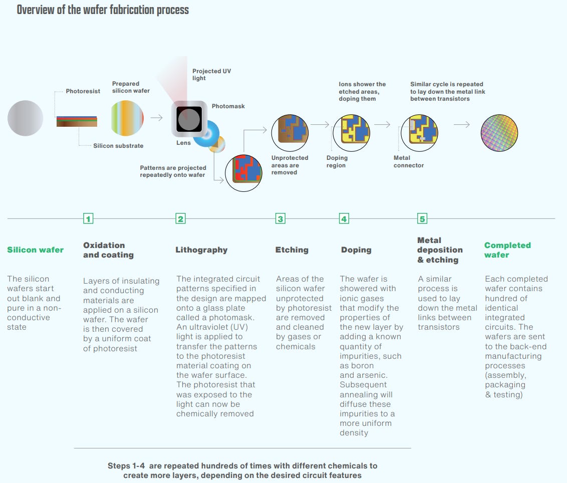
Source: White House report
The lithography machine is the one that does the printing. And the thing that limits how fine a pattern it can print is the wavelength of its light. Shorter wavelength, finer lines. This is intuitive enough: you cannot draw a thin line with a fat marker.
Deep ultraviolet, or DUV, uses light at 193 nanometres. Immersion DUV, the tool in question, is a clever upgrade. You flood the gap between the lens and the wafer with purified water. Water bends light more than air does, which lets the same 193nm source resolve finer features. It is a genuinely difficult machine and it costs around $90 million.
Above that is extreme ultraviolet, or EUV, which uses light at 13.5 nanometres. EUV is what you need for the most advanced chips being made today, the ones inside Nvidia’s accelerators and Apple’s phone processors.
It costs over $200 million a machine, it is roughly the size of a bus, and exactly one company on earth makes it. That company is ASML.
Which brings us to the export controls.
In 2019, the first Trump administration pressured the Dutch government to stop ASML selling EUV to China. Under Biden, the restrictions widened to cover some immersion DUV as well. So Chinese chipmakers did the rational thing and bought as much of the older permitted equipment as they could before the door shut.
One last piece of vocabulary. When people say a chip is made on a “7nm” or “28nm” node, they are not describing a physical measurement any more. Those are generation labels. Smaller number, denser transistors, faster and more power-efficient chip.
Roughly speaking, 28nm and above is “mature” and goes into cars, appliances, power switches and sensors. 7nm and below is “advanced” and goes into flagship phones and AI accelerators.
The obvious and not so obvious readings of the news
Start with capacity, which is where most people jump to.
China already bought the machines it needs.
Ryan Fedasiuk and Julia Torres, in an American Enterprise Institute report from this April, count roughly 90 ArF immersion scanners delivered to Chinese buyers in 2024.
That is $5 billion to $7 billion of tools, all of it landed before the current restrictions bit. Five domestic units a year grows that fleet by about 5 percent. It does not change how many wafers China starts next year.
Then take the frontier reading, that China is closing in on the leading edge. That does not hold either, because SMIC already runs immersion DUV. Its 7nm-class process, the one which is inside Huawei’s Kirin phones and Ascend AI accelerators, gets there through a technique called multi-patterning.
Multi-patterning is worth understanding, because it is the crux of China’s whole position.
If your light cannot print lines fine enough in a single pass, you print half of them, then shift the mask and print the other half in the gaps. Think of drawing fine stripes with a thick marker: you draw every second stripe, then go back and fill in between. It works. SMIC does it three or four times per critical layer. But it has a ceiling, and to get meaningfully denser than SMIC is now you need EUV, which comes from one company and has never shipped to China. So a domestic immersion tool takes China to roughly where it already stands, just slower.
And China is already standing there alone, which is worth noting.
TechInsights teardowns found TSMC 7nm dies inside Huawei’s Ascend 910B and 910C parts, from a stockpile of roughly 2.9 million that Huawei had bought through an intermediary before anyone noticed. TSMC paid a $1 billion fine over it. That stockpile ran out in early 2026, so every Ascend from here comes off SMIC wafers.
The third reading is cost, and here the domestic tool loses outright.
ASML’s NXT:1980Fi pushes 330 wafers an hour, and throughput is most of what you are paying for in a $90 million machine. Nobody outside the programme has seen a throughput figure for the Shanghai tool. The analysts who cover this keep saying the same thing: getting a machine to print once is one problem, getting it to print reliably 24 hours a day for years is a completely different one.
So I think the market got it right, just not for reasons that have anything to do with wafers. China is not buying capacity with these five machines. It is buying back a hostage (more on this later).
The bottleneck has narrowed to two process steps
Here is the thing people miss. Lithography is only one of the 400 to 500 steps. The others matter just as much, and China has spent a decade taking them over.
Briefly, what those steps are.
- Deposition lays down ultra-thin films of metal or insulator across the wafer.
- Etch carves material away through the stencil that lithography printed.
- Cleaning removes contamination between steps, because a single stray particle ruins a chip.
- Planarisation polishes the surface flat again before the next layer goes on.
- Ion implantation fires charged atoms into the silicon to change its electrical behaviour.
- And metrology is the measurement and inspection layer that tells you whether any of it worked.
By the end of 2025, Chinese industry estimates put domestic tool share at roughly 60 percent in etch, 55 percent in deposition, 50 percent in cleaning, 40 percent in planarisation and 30 percent in ion implantation. Metrology sits under 25 percent.
Lithography is basically zero.
The company numbers say the same.
Naura, the largest domestic equipment maker, booked RMB 39.35 billion in 2025, up 31.9 percent. AMEC, which specialises in etch, did RMB 12.39 billion, up 37 percent. Piotech, in deposition, did RMB 6.52 billion, up 59 percent, and then grew another 57 percent in the first quarter of 2026.
Collectively, Chinese equipment vendors held about 1.2 percent of the global market for chipmaking tools in 2021. By 2025 they held 6.5 percent.
And Beijing engineered essentially all of it.
The third National Integrated Circuit Investment Fund, universally called the Big Fund, holds RMB 344 billion and deployed over RMB 164 billion in 2025. Since late 2025, Chinese fabs have had to source at least half the equipment for any new capacity domestically before regulators will sign off on the expansion. SEMI China’s president Lily Feng expects the country’s share of global mature-node capacity to go from 25 percent in 2024 to 42 percent by 2028.
Essentially, this is a country that has closed most of the toolchain and left two doors open: lithography and metrology. And lithography is the one with a single foreign supplier and a US Congress attached to it.
China can already make the chips, it just can’t make them cheaply
Forget nanometres for a second. The gap that actually matters is cost per working chip, and it is huge.
Two things drive that number.
The first is what the wafer costs to run. Chinese research houses price a 28nm wafer at roughly $3,500 and a 14nm wafer at $5,500. At 7nm the numbers split by method: about $8,000 a wafer using EUV, about $10,000 using DUV multi-patterning. Every extra printing pass is extra machine time, an extra mask, and extra handling.
The second is yield, which is the share of chips on a finished wafer that actually work.
This is where the damage happens. You pay for the whole wafer whether or not the chips on it function, so if half of them fail, your cost per working chip doubles. Multi-patterning hurts yield directly, because each additional pass has to line up with the previous one to within a few nanometres.
Analysts estimate SMIC’s N+2 node yields 20 to 40 percent and its N+3 node yields 20 to 30 percent, against TSMC running in the high eighties at the same generation. SMIC’s 5nm-class pilot reportedly sits under 20 percent.
Stack those together and a working SMIC 7nm chip costs two to three times what a TSMC one costs. And that gap is arithmetic, not sloppiness. It does not go away with better management.
You can see the bill in SMIC’s own accounts.
First quarter 2026 revenue came in at $2,505 million, up 0.7 percent sequentially, on a 20.1 percent gross margin and 93.1 percent utilisation. TSMC runs near 60 percent. SMIC spent $8.1 billion on capital expenditure in 2025 and plans something similar this year, ran negative free cash flow, and skipped the 2025 dividend so the cash could stay in the business. Depreciation, which is the accounting cost of all that equipment wearing out, now eats about 44 percent of every revenue dollar, up from 37 to 38 percent a year earlier.
Management does have pricing power right now, to be fair, and guided the second quarter up 14 to 16 percent sequentially at a 20 to 22 percent margin. But that is a shortage helping, not a structural fix.
What you are looking at is a state subsidy running through a listed company. Nobody is paying SMIC to be profitable. They are paying it to exist at 7nm: about 45,000 wafers a month of advanced capacity at the end of 2025, 60,000 targeted this year, 80,000 in 2027.
Five machines buy service independence
In my opinion, you do not really buy a lithography scanner. You subscribe to it.
By now, we know that these machines are not appliances. They need constant recalibration, replacement optics, new light source modules, software updates, and field engineers who know the individual quirks of the individual tool. Left alone, a scanner drifts out of specification and starts producing wafers that fail. ASML books this work as a line called installed base management, and it brought in 2.5 billion euros of the company’s 8.8 billion in the first quarter of 2026. That matters to ASML. It matters far more to the customer.
Now, in April, US lawmakers introduced a bill that would block all ASML immersion DUV sales to China and stop ASML engineers from servicing the tools already sitting there. The second half is the sharp end. Cutting off new sales squeezes slowly. Cutting off service on a fleet of roughly 90 immersion scanners squeezes fast, because those tools are what China’s entire advanced-node production runs on.
That is the hostage.
Five machines a year will not replace the fleet, obviously. What they will do is build what the fleet needs to survive alone: domestic optics, stages, light source components, spare parts, and engineers who have actually integrated an immersion tool from scratch and know where it drifts.
Seen that way, the sell-off makes sense. ASML has already taken the revenue hit. China went from 36 percent of its system sales in the fourth quarter of 2025 to 19 percent in the first quarter of 2026, and management guides to about 20 percent this year against 33 percent in 2025. The leverage was the part still standing. And a domestic tool programme, even a mediocre one, starts spending that down.
Watch throughput, not nanometres
Nobody outside the programme can tell you when China closes this gap, and I certainly cannot.
Masahiro Wakasugi at Bloomberg Intelligence puts lithography parity at seven to ten years, with full equipment replacement further out than that. Reuters reported a domestic EUV prototype back in December. But prototypes are cheap. Fleets are not.
The things worth watching here are boring and countable. Wafers per hour on the Shanghai tool. How well it aligns one printing pass to the next across a full multi-patterning stack. Whether the 20 units promised for 2027 genuinely ship, and whether SMIC runs them in real production or just parks them in qualification. And metrology, the other open door, where localisation still sits under 25 percent, because you cannot fix what you cannot measure.
Export controls stopped being about denying capability a while ago. China can make the chip. It pays two to three times over to do it, and Beijing has shown it will keep paying. What the controls still buy is the ability to switch the tools off.
That is a real asset. It is also a depreciating one.
